Srpski / Arhiva brojeva / DESETI BROJ / dr MILAN L. MAŠANOVIĆ, prof. dr LARRY A. COLDREN: Photonic Device Technology for Coherent Optical Communications, str. 42-52
Photonic Device Technology for Coherent Optical Communications
Milan L. Mašanović, Freedom Photonics LLC and University of California, Santa Barbara
Larry A. Coldren, University of California, Santa Barbara
ABSTRACT
The bandwidth on the optical fiber network is now growing by two orders of magnitude per decade due to the tremendous increase in data transmission, and current WDM systems cannot meet the projected bandwidth demands. As a result, in recent years, first commercial deployments of coherent optical systems have occurred, in order to achieve more spectrally efficient data transmission through existing fiber infrastructure. Photonic integration will play a key role in reaching higher spectral efficiency in a cost efficient, high-performance manner. In this paper, we review the progress and examples of photonic integrated circuits for optical coherent communications. Coherent integrated transmitter and receiver photonic integrated circuits are now a reality, and an active area of research.
Keywords: Photonic integrated circuits, coherent communications, coherent transmitter, coherent receiver, silicon photonics, Indium Phosphide
1. INTRODUCTION
More than three decades since their conception, optical coherent systems are finally a reality. They are being deployed throughout transport optical networks in order to provide more optical bandwidth through existing optical fiber, as well as to simplify dealing with the impairments of transmission, given that in most cases, both optical amplitude and phase are being recovered.
Research on coherent optical technology started in the 1980s because of its promise of increased transmission distance due to improved receiver sensitivity. Er-doped fiber amplifiers (EDFAs) had not been developed at the time, and wavelength division multiplexing (WDM) was expensive due to the repeater cost and complexity (de-multiplexing, optical-electrical conversion, amplification, electrical demultiplexing to a lower data rate, regeneration, multiplexing back up, electrical-optical conversion, and multiplexing into optical fiber).
Coherent approaches have promised to double the repeater separation, and allow placing of the WDM channels closer together, because the channel filtering could be done by a fixed intermediate frequency filter in the RF-domain after heterodyne down-conversion by tuning the optical local oscillator (LO), similar to a radio. Bulk optical heterodyne receivers were quickly found to be very difficult to make due to stability issues. Thus, efforts were initiated early-on to explore the possibility of monolithic integration of Photonic Integrated Circuits (PICs) for coherent communications [1]. However, the invention of the erbium-doped fiber amplifiers and inexpensive, integrated arrayed-waveguide grating-based multiplexers and demultiplexers channeled the development toward modern WDM systems for much of the 1995–2010 timeframe.
WDM systems using amplitude modulation have so far been able to meet the growth of traffic in optical networks, but currently deployed systems and fibers are close to being at full capacity. The traffic on the optical fiber network is now growing by two orders of magnitude per decade due to the tremendous increase in data transmission. The aggregate optical network traffic, both historic and predicted, is shown in Figure 1.
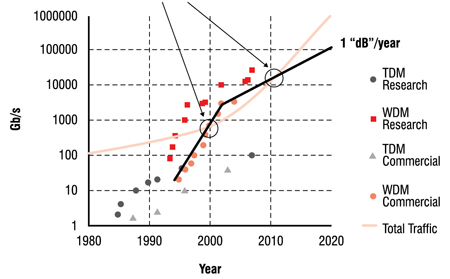
Figure 1. Historic and predicted optical network traffic growth as function of time
Therefore, it is a continuing challenge to meet the future demand for bandwidth. Figure 1 overlays some data for fiber capacity on this total demand curve for both research and commercial fiber links [1]. The straight lines indicate trends for commercial systems, which show that the tremendous growth in bandwidth, due to WDM adoption in the 1995-2002 timeframe, has nowreached saturation due to the limitation in the number of practical WDM channels, as well as the data rate in each of them. In order to further increase the fiber capacity, we are either looking at the expensive proposition of laying more optical cables, or at improving the net data rate per Hz of bandwidth —spectral efficiency (SE), or, more simply, the channel rate/channel spacing ratio in existing fibers. This is being done using advanced (phase) optical modulation formats and coherent detection.
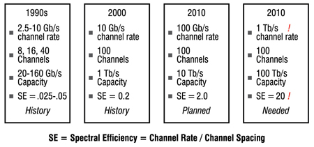
Figure 2. Optical system evolution in terms of bandwidth and spectral efficiency, past and future.
Figure 2 gives a set of tables that summarize the system evolution over the past few decades, as well as what a simple extrapolation might predict for the next decade [3].
As might be immediately obvious, an extrapolation of the current rapid growth in fiber capacity does not meet the network demand by 2020, even if doubled or tripled by using the fiber S and L bands in addition to the standard C-band which is plotted in Fig. 2. Even worse, calculations show that we will never be able to reach SE = 20 due to limitations in fiber dynamic range because of its limited power handling capacity [4]. A spectral efficiency of ~ 10 seems more realistic for transmission distances ~ 100 - 500 km, typical of WDM systems.
The need for improving the spectral efficiency of transmission in the future has led to renewed interest and intense research on optical coherent systems, as well as to the recent deployments of this technology. Coherent optical communications rely on digital modulation, a term used in radio, satellite, and terrestrial communications to refer to modulation in which digital states are represented by modification of carrier amplitude, frequency, and phase, simultaneously or separately. A common name for this arbitrary carrier phase and magnitude modulation is vector modulation. Different modulation states are represented by components of the electric field vector in the complex plane, using in-phase and quadrature (I-Q) constellation diagrams, illustrated in Figure 3. for three different modulation formats. In optical communication systems, the carrier frequency (laser wavelength) is usually fixed; thus we only need to consider the phase and magnitude changes. The unmodulated carrier is then the phase and frequency reference, aligned along the I axis, and the modulated signal is interpreted relative to the carrier. Q represents the quadrature (90◦ out of phase) vector component. A discrete point, modulation state on the I-Q diagram, can be represented by vector addition of a specific magnitude of the in-phase carrier with a specific magnitude of the quadrature carrier.
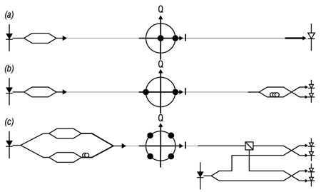
Figure 3. (a) Amplitude modulation (on-off keying) based noncoherent system with direct detection (b) Differential phase shift keying based coherent system with self-homodyne detection, without the need for a local oscillator (c) Quadrature phase shift keying coherent system with intradyne coherent detection, using a local oscillator matched in frequency and phase to the input signal.
Figure 3. illustrates some of the unique, commonly used vector modulation based links. The first link, part (a), utilizes simple binary amplitude modulation, the most widely exploited, noncoherent modulation format in optical communications to date. On the I-Q diagram, the field vector changes its amplitude from 0 to the maximum amplitude, along the I axis, as binary digital signals are translated into a stream of light pulses. The transmitter in this case is a simple amplitude modulator, and signal detection is achieved through direct detection, as shown in the link schematic.
Link (b) represents the next level of sophistication — a simple coherent system, in which the amplitude of the signal remains constant, but the phase of the carrier is differentially changed by π in between bits, to reflect the change in adjacent bit value. To detect this type of signal, one approach is differential detection, where the signal is interfered with its own delayed version to produce an amplitude response at the receiver. No local oscillator is required in the receiver in this case. This system is limited to a particular bit rate, as it relies on exactly one bit delay for signal detection. Note that the receiver consists of two photodiodes that are connected in series, forming a balanced receiver, examined later in this section.
Figure 3. (c) illustrates a more complex and flexible system, where the carrier phase is modulated to one of four possible values — thus the name of this type of modulation is quadrature phase shift keying (QPSK). The advantage of this approach is in the fact that with the same bit rate as on-off keying, we can transmit twice the amount of information, since with each detected symbol (1 out of 4 possible phase values), we can recover two bits of information, a major benefit of vector modulation and coherent systems. The transmitter for this modulation format is relatively simple, consisting of two nested Mach-Zehnder phase modulators, which are delayed by 90◦ with respect to one another, allowing independent I and Q component modulation. The main complexity results from the receiver, where the incoming signal needs to be phase matched, locked and mixed with a local oscillator laser. In addition, the signals in the receiver need to be mixed and delayed properly, so that both the I and the Q signal components can be extracted independently, in the two sets of balanced receivers shown in the schematic. Any changes in phase of the incoming signal, caused by the laser phase noise, need to be tracked and neutralized in the receiver. A number of different techniques can be used to accomplish this. Optical phase-locked loops use optical feedback to control the phase of the local oscillator laser [5], showing promise for low power, simple implementation of true coherent receivers. Digital signal processing can be used to perform real time phase tracking and control as well, at the expense of electronic chip sophistication and power consumption [6].
Although these three examples show the progression from simple, noncoherent amplitude modulated system, through a differentially modulated coherent system to a true I-Q coherent system, it is important to emphasize that many other different vector modulation formats and links are possible and used: differential QPSK, where the phase changes to one of four states are recorded only when the adjacent bit changes; or quadrature amplitude modulation (QAM), where both the amplitude and the phase of the I and Q components are changed, resulting in a multitude of points on the constellation diagram, and further improvement of spectral efficiency, up to the fundamental limit imposed by the fiber dynamic range to around 10 bits/s per Hz of bandwidth. Finally, additional doubling in spectral efficiency for each of the coherent links can be accomplished by multiplexing two signals onto two degenerate orthogonal polarizations of an optical fiber, creating a polarization-multiplexed (PM) link.
2. COHERENT OPTICAL TRANSMITTERS COMPONENTS
As discussed in the previous section, arbitrary vector modulation can be generated using the combination of both amplitude and phase modulation. One popular way to accomplish this task is to use the nested Mach-Zehnder modulator structure shown in Figure 3. (c). Because this structure assigns the I axis to one MZM and the Q axis to a second MZM, it can modulate the resultant vector to any (I,Q) point in the plane of the I-Q diagram. For QPSK modulation, four equal amplitude (I-Q) points are accessed.
An example of dual polarization, indium phosphide (InP) based QPSK modulator fabricated by NTT is shown in Figure 4. The InP dual, nested Mach-Zehnder modulator PIC has a single TE input and two individual output ports. The PIC is packaged on a carrier with a Silica based planar lightwave circuit (PLC) whose function is to couple the light from both PIC’s outputs, to rotate the polarization from one of the PIC’s outputs, and then to combine two polarizations in a single output waveguide. A special, high-speed interposer is used on top of the modulator to provide high-speed electrical connections for 112 Gbps operation [7].

Figure 4. Configuration on an InP-based dual polarization QPSK modulator by NTT [7]. The solution consists of a dual modulator, dual output InP chip, microoptics, high-speed electrical imposer, and a PLC.
A 10-wavelength transmitter PIC by Infinera, utilizing a type of a nested I-Q Mach-Zehnder structure for QPSK modulation is shown in Figure 5[8]. Polarization multiplexing is implemented in this example to double the transmission rate, requiring a pair of identical nested I-Q MZ structures for each of the 10 DFB lasers on the chip. The constellation diagrams in the figure illustrate the four constellation points accessed by each of the 20 I-Q modulators. Each individual I and Q MZ modulator is running at 14.25 Gbps, but as discussed above with QPSK modulation, we double the amount of information transmitted (by effectively combining the I and Q signals in phase quadrature) resulting in 28.5 Gbps per IQ modulator. This chip utilizes DFB lasers for the light source, but one could imagine replacing them with the widely tunable variety.
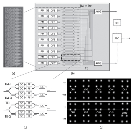
Figure 5. (a) Photograph of the active block of a 10-wavelength PM-QPSK transmitter IC, utilizing nested IQ Mach-Zehnder modulator, DFB-laser devices, (b) schematic layout of PIC illustrating the TE and TM-to-be duplicate sets of modulators, AWGS, and output waveguides, to support polarization-multiplexed operation through off-chip polarization beam combining, (c) schematic of TE/TM nested IQ MZ modulator section of one wavelength showing RF and DC controls, and (d) IQ constellation diagrams for all 20 QPSK data streams, each IQ stream running at 28.5 Gbps for an aggregate 570 Gbps transmission capability across the 10 wavelengths [8].
The first such chip, reported in [9], consists of a widely-tunable sampled-grating DBR (SGDBR) laser monolithically integrated with a nested Mach-Zehnder modulator, as shown in Figure 6.
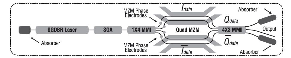
Figure 6. Schematic of a tunable monolithic photonic coherent transmitter, including SOAs, nested MZMs, and absorbers by Freedom Photonics [9].
The chip was realized using monolithic integration in Indium Phosphide (InP) based on quantum well intermixing. The single-mode SGDBR laser provides 40 nm of tuning around 1550 nm. The signal from the laser is amplified with a semiconductor optical amplifier (SOA), and then split into 4 paths, using a 1x4 multimode interference (MMI) splitter. The light in each path is sent through a static phase adjustment electrode embedded in the S-bend waveguides, which is essential for setting the MZMs in the quadrature state. The high-speed MZMs are formed using 400 μm long quantum-well intermixed (QWI) regions, with a photoluminescence (PL) peak at 1.5μm, utilizing the quantum-confined Stark effect (QCSE) for light absorption. After the light in each of the four arms is modulated, it is recombined in a 4x3MMI, which allows for monitoring of the MZM in the OFF state. Thus, the chip is capable of transmitting a single transverse-electric (TE) polarization QPSK data stream in a compact footprint. The key issue with tunable laser integration for coherent transmitter purposes is that of achieving sufficiently narrow linewidth and low phase noise, and this will remain the area of active research in the near future.
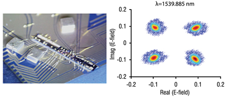
Figure 7. (left) Photograph of the widely tunable optical transmitter integrated circuit mounted on an Aluminum-Nitride ceramic carrier. (right) A representative constellation diagram from coherent link demonstration using a 20 Gbps QPSK encoded optical signal with 231-1 PRBS, after DSP post processing. Linear color coding corresponds to symbol density.
Different integrated modulator configurations in addition to the nested MZMs can be used to generate QPSK and even more advanced modulation formats. Figure 8 shows a DQPSK modulator that uses two asymmetrical STAR couplers in a three-branch interferometer configuration. Two of the three branches contain electroabsorption modulators, which, when biased OFF, ON, and alternatively ON and OFF generate the 4- phase modulated constellation [10]. Also shown is the demodulated result at 20 Gb/s for one of the I or Q outputs.
3. COHERENT RECEIVER IMPLEMENTATIONS
The key idea behind coherent detection is to combine the input signal coherently with a locally generated continuous optical field (local oscillator) at the receiver and before the signal is detected. This action achieves two effects: it amplifies the detected signal through mixing with a high-power local oscillator signal, allowing improved receiver sensitivity, and it enables the demodulation of phase and amplitude/phase modulated signals, which is not possible through direct detection. This is a key enabler for achieving improved spectral efficiency in a coherent link.

Figure 8. A DQPSK electroabsorption modulator photo, schematic, and received signal at 20 Gbps [10] by Bell Labs.
A couple of different coherent receiver architectures, for differential and regular detection were described in Figure 3. Since dual-polarization, dual-quadrature (DPDQ) coherent receiver requires many components, they should ideally be implemented as photonic integrated circuits (PIC). From the technological standpoint, this can be accomplished using a variety of integration platforms, starting from monolithic integration in Indium Phosphide, through hybrid integration using Silica or polymer waveguides, to Silicon photonics.
An example of a high-speed, integrated I-Q receiver in InP is shown in Figure 9. This device consists of two optical spot-size converters, input waveguides, a 90◦ hybrid implementation using a 2 × 4 multimode interference coupler, and two balanced photodiode pairs. The optical hybrid allows for mixing of the local oscillator L and the input signal S, and for balanced detection of both the in-phase I and the quadrature Q components of the input signal. This is accomplished through precise phase control in signal splitting, which results in the following signal combination at each of the photodiodes in Figure 9, from top down, assuming that the signal S is coupled to the top input waveguide: L + S , L − S , L + jS and L − jS . The outputs from two balanced receiver pairs will be 2S and 2jS, the in-phase and quadrature components of the input signal.
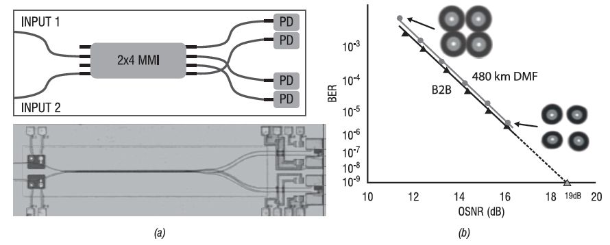
Figure 9. An integrated I-Q receiver in InP (a) Receiver architecture schematic, showing two inputs, a 90◦ hybrid implementation using a 4 × 4 MMI coupler, connected to two balanced photodiode pairs; a device photograph on the bottom. (b) Results of receiver operation at 50 Gbps, showing the bit error rate and constellation diagrams as function of optical signal to noise ratio [11].
This type of I-Q receiver chip can be used in a polarization diversity configuration, with additional micro-optics, to yield a full coherent receiver. A 100 Gbps polarization multiplexed BPSK and QPSK receiver architecture using the InP chip from Figure 9 and actual module are shown in Figure 10. Both the signal and the local oscillator (LO) are coupled through a collimator (C), and a first half waveplate (HWP) is inserted in the optical path in order to evenly split the LO signal between two polarizations. Both signals are split into two polarizations using a polarization beam splitter. To achieve highest symmetry in both channels, X and Y, a second HWP is integrated in the X channel to perform a TM-to-TE conversion. In return and to minimize the channel path length difference a skew compensator (SC) is integrated in the Y channel. The four beams are then coupled through a micro-lens array into the integrated optical spot size converters of the two InP I-Q receiver PICs. Four linear differential trans-impedance amplifiers (TIAs) are co-packed in the module.
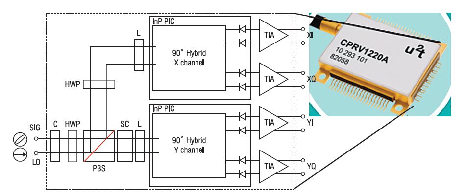
Figure 10. Architecture and module of a 100 Gbps coherent receiver [12] based on the InP PIC from Figure 9, and marketed by U2T.
Another integration platform concept for polarization-diversity receiver modules is polymer waveguide based, since it allows for low-loss, low-cost, simple processing implementation. One obvious challenge for this platform was the integration of photodiodes with minimal insertion loss. In the recent work reported in [13], this has been accomplished by integrating III-V active components via 45˚ turning mirrors, as shown in Figure 11. Also shown is the measured receiver performance in terms of the small signal bandwidth.
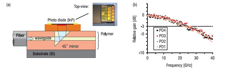
Figure 11. Detail of a Heinrich Hertz Institute’s polymer based coherent receiver implementation, showing the photodiode coupled to the polymer waveguide via a 45 degree mirror [13].
Recent advances in silicon photonics have made realization of complex, high-performance PICs in silicon a reality. Silicon material system realization is beneficial because of the availability of 200-mm diameter or larger optical wafers allowing for low-cost chips. Silicon chips do not require a hermetic environment, allowing for low-cost packaging, and silicon can be oxidized allowing for high vertical index contrast and consequently high-performance polarization splitters and on-wafer testing.
An example of a Si DPDQ coherent receiver [14] is shown in Figure 12. The signal and local oscillator (LO) enter the PIC through 2-D grating couplers spaced by 127 μm. A key novel feature of this device is that grating couplers serve as spot-size converters, polarization splitters, and 50/50 splitters, they do not require anti-reflection coatings and allow for on-wafer testing. A scanning electron micrograph (SEM) of one of the fabricated grating couplers is shown the bottom of Figure 12. The fiber is oriented exactly vertically, i.e. no tilt angle, which results in the grating coupling equally to both directions in the waveguide and thus acting as a 50/50 coupler. After the grating couplers, portions of the LO and signal pass through a 90˚, 11 μm wide waveguide crossing. The wide waveguide renders the crossing loss and crosstalk negligible.
The LO and signal portions pass by directional couplers which couple away any stray transverse-magnetic polarized light. The portions then interfere in four large 2x2 multimode interference (MMI) couplers (the large size improves fabrication tolerance). The MMI coupler outputs connect to eight photodiodes (PDs). The PDs are Ge-on-Si vertical PIN diodes.
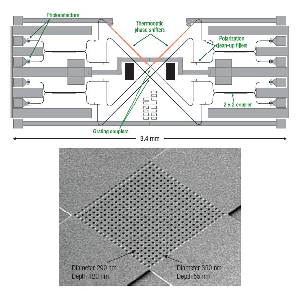
Figure 12. (top) Layout of a polarization multiplexed silicon photonics coherent receiver PIC, consisting of grating coupler inputs and two sets of I-Q balanced receivers. The waveguides are shown as black, the thermooptic phase shifters orange, and the top metal blue. (bottom) Input grating coupler close-up. This novel grating coupler serves as spot-size converter, polarization and 50/50 splitter [14]
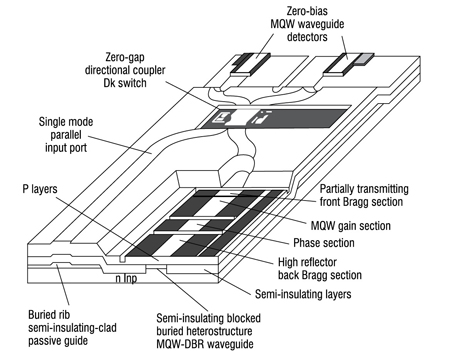
Figure 13. Schematic diagram of a Bell Labs MQW balanced heterodyne receiver photonic integrated circuit, containing a continuously tunable LO, a low-loss buried-rib parallel input port, an adjustable 3 dB coupler, and two zero-bias MQW waveguide detectors [1].
None of the implementations discussed so far include integration of the local oscillator with the receiver. A basic coherent receiver implementation with an integrated local oscillator [1], a historic example of one of the first complex PICs realized is shown in Figure 13. It consists of a DBR laser, light coupler, and a balanced receiver pair on the detection side. The local oscillator signal and the input signal are mixed inside a 2 × 2 coupler element, and detected by two individual photodiodes, connected in series. With this photodiode configuration and the phase differences introduced by the optical coupler, it is possible to easily obtain an output signal which will be given by the difference of the two photocurrents, thereby canceling out the current contributions and the intensity of noise from the local oscillator, and adding the photocurrents resulting from the signal modulation. This type of architecture therefore allows for complete rejection of the CW signal, and conversion of phase modulation into amplitude modulation.
As with coherent transmitters, integration of a widely tunable local oscillator would further benefit the level of integration in coherent receiver PICs. The first implementation of an integrated widely tunable coherent receiver, reported by Freedom Photonics, is shown in Figure 14[15]. The chip was realized using photonic integration in Indium Phosphide. At the center of the chip is a widely tunable sampled grating distributed Bragg reflector (SGDBR) laser, used as the receiver LO, providing 40nm tunability and bandwidth coverage. The signal from the LO is split into two identical paths. In each of the two paths, the LO power is amplified with a semiconductor optical amplifier (SOA), before the signal is routed using 2 total internal reflection (TIR) mirrors with a perpendicular waveguide connecting them. The signal from the second TIR mirror is then guided into a 2x4 multimode interference (MMI) hybrid. The receiver chip has two signal input waveguides, which are used to independently couple each of the two demultiplexed polarization data streams from a polarization multiplexed network data stream. The four outputs of each of the hybrids are separated using S-bend waveguides, which terminate in 4 photodiodes. Thus, the chip is capable of simultaneously detecting two independent data streams from a polarization multiplexed QPSK data stream – however, polarization demultiplexing and rotation of the transverse-magnetic (TM) polarization into transverse-electric (TE) has to be performed external to the chip.
Error-free, 20Gbps (10Gbaud) operation with this chip has been demonstrated. Recently, a similar device has been reported as part of an optical phase locked loop, for homodyne coherent detection, which was discussed as an alternative to high power consumption digital signal processing based detection methods [5].
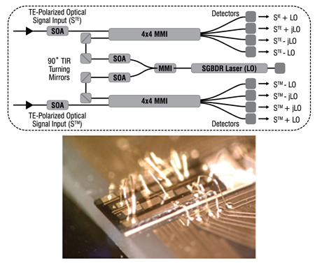
Figure 14. (top) Schematic of Freedom Photonics’ monolithically integrated dual-polarization tunable photonic integrated coherent receiver, including SOAs, MMIs and total internal reflection mirrors and a tunable local oscillator laser. (bottom) Photograph of the widely tunable optical receiver integrated circuit mounted on a ceramic carrier [15].
4. CONCLUSIONS
The bandwidth on the optical fiber network is now growing by two orders of magnitude per decade due to the tremendous increase in data transmission, and current WDM systems cannot meet the projected bandwidth demands. As a result, in recent years, first commercial deployments of coherent optical systems have occurred, in order to achieve more spectrally efficient data transmission through existing fiber infrastructure. Photonic integration will play a key role in reaching higher spectral efficiency in a cost efficient, high-performance manner. In this paper, we have discussed the progress and examples of photonic integrated circuits for optical coherent communications. Both integrated transmitters and receiver PICs are now a reality, but this will remain an active research area for the foreseeable future. Some of the key challenges to be solved are with low phase noise tunable laser integrated technology, higher efficiency modulators, and reduced footprint receivers integrating polarization splitting on chip.
References
[1] Koch TL, Koren U, Gnall RP, Chao FS, Hernandez-Gil F, Burrus CA, Young MG, Oron M, Miller BI., “GaInAs/GaInAsP multiple-quantum-well integrated heterodyne receiver”, Electron Lett 1989;25: 1621.
[2] L. A. Coldren, S. C. Nicholes, L. Johansson, S. Ristic, R. S. Guzzon, E. J. Norberg, U. Krishnamachari, “High Performance InP-based Photonic ICs—a Tutorial”, IEEE Journal of Lightwave Technology, 2011
[3] R. Tkach, “Optical Network Capacity: From Glut to Scarcity,” OIDA Annual Meeting, Santa Clara, CA, Dec. 1-2, 2009.
[4] R. Essiambre, et al, in talk by R. Alferness, “Optical communications—a view to the future,” ECOC’08, Brussels, Sept. 2008. See also, R.-J. Essiambre, G. Kramer, P. J. Winzer, G. J. Foschini, and B. Goebel,"Capacity limits of optical fiber networks," J. Lightwave Technol.,vol. 28, pp. 662-701, 2010.
[5] M. Lu, H. Park, E. Bloch, A. Sivananthan, J. Parker, Z. Griffith, L. A. Johansson, M. J. Rodwell, and L. A. Coldren, “A Photonic Integrated Circuit for a 40 Gbaud/s Homodyne Receiver Using an Optical Costas Loop”, IEEE Integrated Photonics Conference, 2012.
[6] O’Sullivan M. “Expanding network application with coherent detection” National Fiber Optic Engineers Conference; 2008.
[7] Yamada, E.; Kanazawa, S.; Ohki, A.; Watanabe, K.; Nasu, Y.; Kikuchi, N.; Shibata, Y.; Iga, R.; Ishii, H.; , "112-Gb/s InP DP-QPSK modulator integrated with a silica-PLC polarization multiplexing circuit," Optical Fiber Communication Conference and Exposition (OFC/NFOEC), 2012
[8] Evans P, et al, “Multi-channel coherent PM-QPSK InP transmitter photonic integrated circuit (PIC) operating at 112 Gb/s per wavelength”, Optical Fiber Communication Conference, Post Deadline Paper PDPC7; 2011 March.
[9] Estrella, S.B.; Johansson, L.A.; Masanovic, M.L.; Thomas, J.A.; Barton, J.S.; , "First Monolothic Widely Tunable Coherent Transmitter in InP" Photonics Technology Letters, IEEE, submitted for publication
[10] Doerr, C.R.; Zhang, L.; Winzer, P.J.; Sinsky, J.H.; Adamiecki, A.L.; Sauer, N.J.; Raybon, G.; , "Compact High-Speed InP DQPSK Modulator," Photonics Technology Letters, IEEE, vol.19, no.15, pp.1184-1186, Aug.1, 2007
[11] Bottacchi S, Beling A, Matiss A, Nielsen ML, Steffan AG, Unterborsch G, Umback A. “Advanced photoreceivers for high-speed optical fiber transmission systems. IEEE Journal of Selected Topics in Quantum Electronics 2010;16(5): 1099–1112.
[12] Matiss, A.; Nolle, M.; Fischer, J.K.; Leonhardt, C.C.; Ludwig, R.; Hilt, J.; Molle, L.; Schmidt-Langhorst, C.; Schubert, C.; , "Characterization of an integrated coherent receiver for 224 Gb/s polarization multiplexed 16-QAM transmission," Optical Fiber Communication Conference and Exposition (OFC/NFOEC), 2011 and the National Fiber Optic Engineers Conference , vol., no., pp.1-3, 6-10 March 2011
[13] Wang, J.; Kroh, M.; Richter, T.; Theurer, A.; Matiss, A.; Zawadzki, C.; Zhang, Z.; Schubert, C.; Steffan, A.; Grote, N.; Keil, N.; , "Hybrid-Integrated Polarization Diverse Coherent Receiver Based on Polymer PLC," Photonics Technology Letters, IEEE , vol.24, no.19, pp.1718-1721, Oct.1, 2012
[14] Doerr, C.R.; Buhl, L.L.; Baeyens, Y.; Aroca, R.; Chandrasekhar, S.; Liu, X.; Chen, L.; Chen, Y.-K.; , "Packaged Monolithic Silicon 112-Gb/s Coherent Receiver," Photonics Technology Letters, IEEE , vol.23, no.12, pp.762-764, June15, 2011
[15] Estrella, S.B.; Johansson, L.A.; Masanovic, M.L.; Thomas, J.A.; Barton, J.S.; , "Widely Tunable Compact Monolithically Integrated Photonic Coherent Receiver," Photonics Technology Letters, IEEE , vol.24, no.5, pp.365-367, March1, 2012
Authors
Dr. Milan L. Masanovic (S’98–M’04) received the Dipl. Ing. degree from the School of Electrical Engineering, University of Belgrade, Belgrade, Yugoslavia, in 1998 and the M.S. and Ph.D. degrees from the University of California Santa Barbara, in 2000 and 2004, respectively, all in electrical engineering. He is currently a General Manager at Freedom Photonics LLC, a Santa Barbara based photonic integration company, as well as a Research Scientist at the University of California Santa Barbara. He has co-authored of more than 85 journal and conference papers, and presented numerous invited talks at international conferences. His current research interests include InP photonic integrated circuits (diode lasers and tunable transmitters), component technologies for packet-switched optical networks, local area networks and harsh environments. Dr. Masanovic was the recipient of a number of merit based awards, including the 2004 IEEE Lasers and Electro-Optics Society Fellowship Award. He has taught graduate level course on semiconductor lasers and photonic integrated circuits at UCSB in 2009, 2010 and 2011, and has served as a reviewer for a number of journals, and on technical committees for Integrated Photonics Research conference, Indium Phosphide and Related Materials conference, Microwave Photonics conference, and Avionics, Fiber Optics and Photonics conference.
Dr. Larry A. Coldren (S’67–M’72–SM’77–F’82) received a Ph.D. degree in electrical engineering from Stanford University, Stanford, CA, in 1972.
He is the Fred Kavli Professor of Optoelectronics and Sensors at the University of California, Santa Barbara (UCSB). After 13 years in the research area at Bell Laboratories, he joined UCSB in 1984, where he now holds appointments with the Department of Materials and the Department of Electrical and Computer Engineering. In 1990, he cofounded Optical Concepts, later acquired as Gore Photonics, to develop novel VCSEL technology, and, in 1998, he cofounded Agility Communications, later acquired by JDSU, to develop widely-tunable integrated transmitters.
At Bell Labs, he initially worked on waveguided surface-acoustic-wave signal processing devices and coupled-resonator filters. He later developed tunable coupled-cavity lasers using novel reactive-ion etching (RIE) technology that he created for the then new InP-based materials.
At UCSB, he continued work on multiple-section tunable lasers, in 1988 inventing the widely-tunable multi-element mirror concept, which is now used in some JDSU products. Near this same time period, he also made seminal contributions to efficient vertical-cavity surface-emitting laser (VCSEL) designs that continue to be implemented in practical devices to this day. More recently, his group has developed high-performance InP-based photonic integrated circuits (PICs) as well as high-speed VCSELs, and they continue to advance the underlying materials growth and fabrication technologies. He has authored or coauthored over a thousand journal and conference papers, seven book chapters and one textbook and has been issued 64 patents. He has presented dozens of invited and plenary talks at major conferences.
Prof. Coldren is a Fellow of the IEEE, OSA, IEE, and a member of the National Academy of Engineering. He was a recipient of the 2004 John Tyndall and 2009 Aron Kressel Awards.